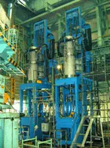
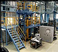
Compound Semiconductor Single Crystal Manufacturing Equipment
To achieve higher performance and lower cost, the compound semiconductor crystal must have a lower dislocation density and a larger diameter. In response to the demand, we have developed single crystal manufacturing equipment using the high pressure vertical Bridgman (VB) method.
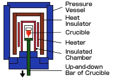
VB Method
| Maximum temperature | 1650℃ |
|---|---|
| Maximum pressure | 9.8MPa (100kgf/cm2) |
| Crucible dimensions | Φ2 inches X 150mmL |
| Heater type | 6-Zone highly purity graphite heater |
| Pressure support system | Press frame |
Examples of Application
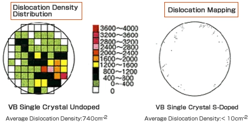
This equipment is suitable for manufacturing of various compound semiconductors including GaAs, GaP and InP (Group III-V) and ZnSe (Group II-VI). The following figure gives an example of the dislocation density distribution of GaP single crystal. It has been reduced to 740 cm-2 for undoped semiconductors and 10cm-2 or less for S-doped, which result in less than 1% compared with the conventional equipment (LEC).
| Growth Conditions | |
|---|---|
| Crystal size | 2 inches |
| Crystal growth orientation | <100> and <111> |
| Dopant | S-Doped, Undoped |
| Pressure | 7.8 MPa (Argon Gas) |
| Growth rate | 3 mm/hr |
Dislocation Density Distribution of GaP Single Crystal
We also design and manufacture other equipment such as annealing furnaces, material synthesis apparatuses and ultrahigh pressure single crystal manufacturing equipment (1 GPa-class).
Contact Us
You can reach us by clicking the inquiry button.