Sputtering targets for oxide semiconductors
The oxide semiconductor material with higher electron mobility than IGZO
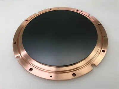
The Material Business of Kobelco Research Institute, Inc. introduces oxide semiconductor sputtering targets for Φ300mm Si wafers.
This material is an oxide semiconductor realized by our own development, showing higher electron mobility and higher TFT reliability than conventional oxide semiconductor (IGZO), and has already been widely adopted in flat panel display application.
In silicon semiconductor uses, this material has been applied to embedded memory devices for R&D, and improvement in the memory operation has been confirmed. KOBELCO proposes this material to contribute to the functional improvement of future edge devices and for the social implementation of artificial intelligence.
Responsible Company: Kobelco Research Institute, Inc. (Japanese site)
Features
- Electron mobility of KOS-B03C is higher than that of a-Si and IGZO.
Minimization of oxide transistor size can be realized. - Low temperature process is possible.
Oxide transistor can be formed during back-end process. - Wide band-gap semiconductor film is deposited by DC sputtering
Transparent transistor can be formed directly on a transparent film. - Leakage current of oxide transistor is quite lower than that of the others.
Hybrid device with c-Si and oxide transistors leads to electric power saving.
| Thin-film semiconductor material | a-Si | LTPS (low temperature poly-Si) |
Oxide |
|---|---|---|---|
| Electron mobility (cm2/Vs) | 0.5 - 1 | 60 - 100 | IGZO:10 KOS-B03C:20-30 |
| Deposition method | CVD | CVD & Laser Anneal | DC Magnetron Sputtering |
| Large area | Possible | Impossible | Possible |
| Process temperature(℃) | < 350 | < 600 | < 350 |
| Band gap(eV) | 1.4 - 1.8 | 1.1 | 2.9 - 3.3 |
| Off leakage current(A/mm) | 1×10-13 | 1×10-12 | 1×10-16 |
Characteristics
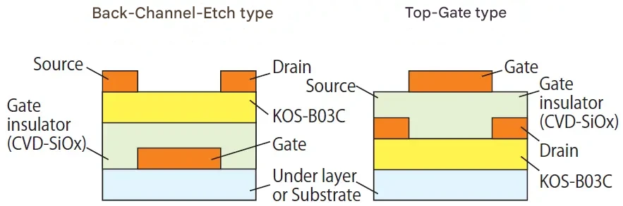
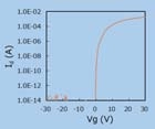
| Back-Channel-Etch type | Top-Gate type | |
|---|---|---|
| Transfer curve |
 |
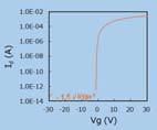 |
| Saturation mobility | 29.1cm2/Vs | 24.4cm2/Vs |
| Vth | 0.50V | -0.75V |
| S.S. | 0.17V/dec. | 0.16V/dec. |
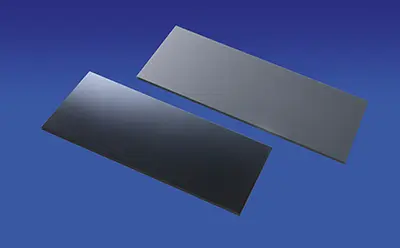
Product line-up
Sputtering targets with various sizes and shapes are available.
Contact Us
You can reach us by clicking the inquiry button.