Semiconductor wafer inspecting devices
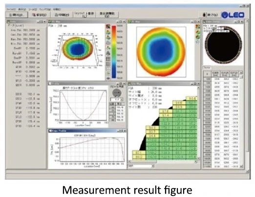
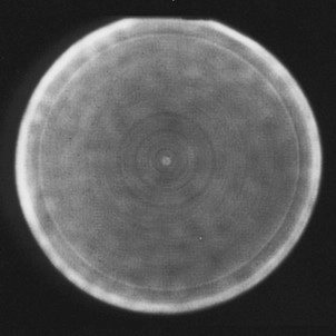
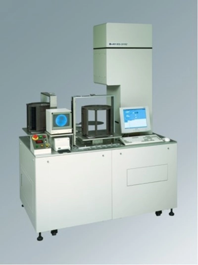
Flatness Measurement System (For Sliced, Rapped and Ground Wafer, For Polished Wafer)
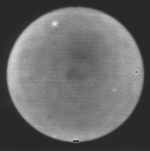
The flatness and shape of wafers are measured with high precision
A range of flatness measurement system is available, from line-scanning type (SBW series) to ultrahigh precision models capable of measuring site flatness (LSW series), and the LNSW series with a nanotopography function for inspecting shipments.
Responsible Company: Kobelco Research Institute, Inc.
Measurement examples
Product line-up
SBW series
- Features
-
- With our unique measurement method, thickness variation, bow, and warp can be measured with high precision with a simple configuration.
- In accordance with the measuring object, the method can be selected from capacitive sensing method, laser displacement meter method, or other methods.
- Usage
-
- On-site control of flatness and warp after slicing, grinding, etching, and polishing.
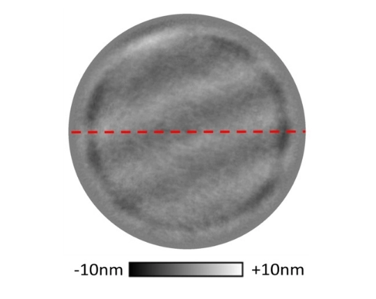
LSW, LNSW series
- Features
-
- Reproducibility at the sub-nano level is realized by our own developed super-precision heterodyne Interferometer.
- Global flatness (such as GBIR), site flatness (such as SFQR), bow, and warp can be measured.
LNSW can measure nanotopography.
- Usage
-
- High precision flatness measurement after polishing and inspection when shipping
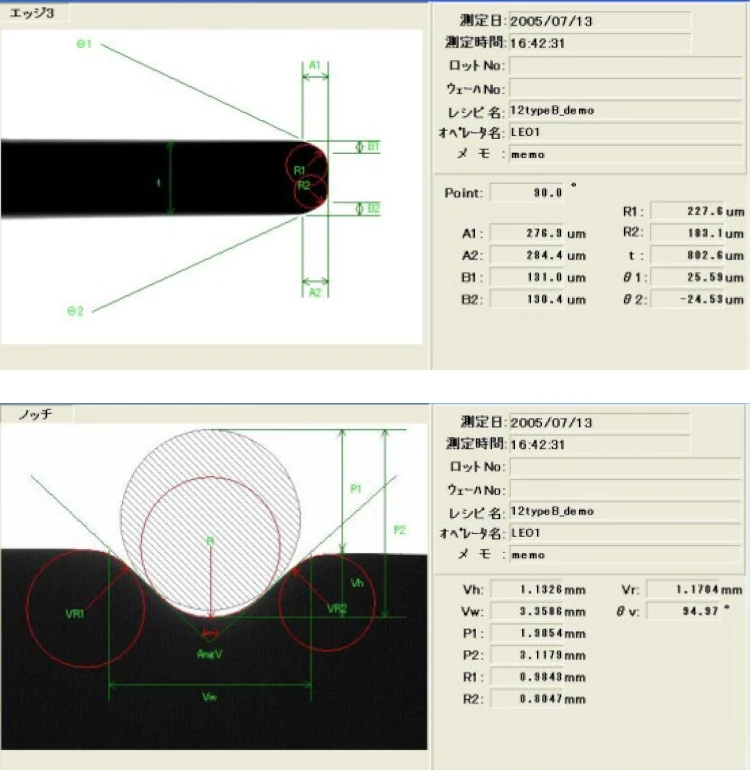
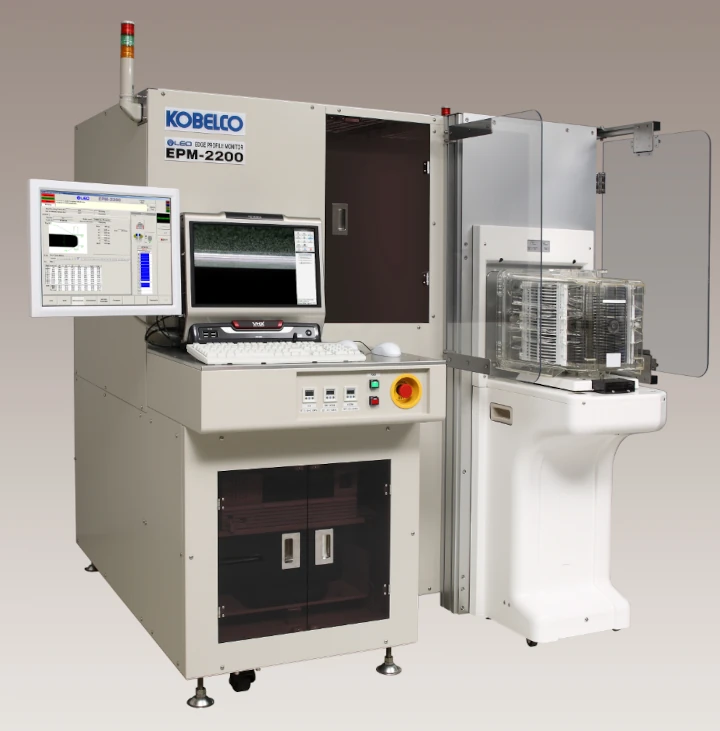
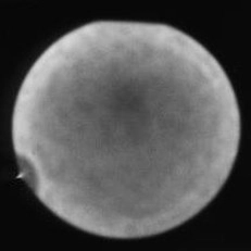
Edge-related inspection devices (edge shape, bonding misalignment, and chipping)
The shapes of edges and notches are measured with high precision by our unique optical image processing technologies.
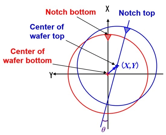
With the LEP series, the chamfered shape, orientation flat length, diameter, thickness, notch shape, etc. of wafers can be automatically measured without contact. In addition to this, the EMB series can measure wafer bonding misalignment, and the LEI series can inspect chipping.
Responsible Company: Kobelco Research Institute, Inc.
Measurement examples
Product line-up
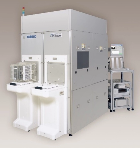
LEP series
- Features
-
- Edge shape can be measured with high precision by our unique algorithm.
- Usage
-
- Quality confirmation immediately after edge processing, shipment inspection, performance confirmation of processing machines, etc.
EPB series
- Features
-
- Owing to edge measurement technologies and notch position measurement, bonding misalignment of wafers without an alignment mark can be measured.
- Usage
-
- Inspection in the bonding process, etc.
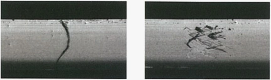
LEI series
- Features
-
- Fine images of a wafer’s entire circumference obtained by a high sensitivity line scanning camera can be stored.
- Usage
-
- Detection of defects (chip), cracks, and scars formed in the wafer edge portion, and judgement of acceptable/unacceptable
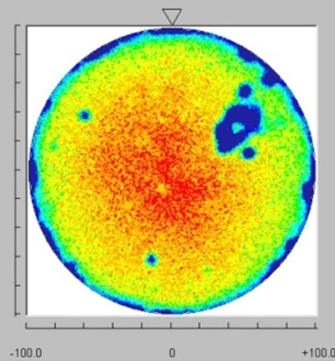
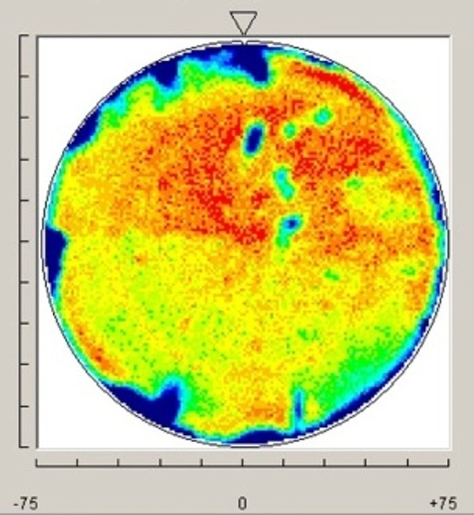
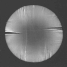
List of life time measuring devices
Life time of carrier recombination is measured.
Life time is an important parameter strongly affected by contaminants in the sample, crystal defects, etc.
Responsible Company: Kobelco Research Institute, Inc.
Measurement examples
Decrease in the life time due to wafer contamination (blue portion)
Product line-up
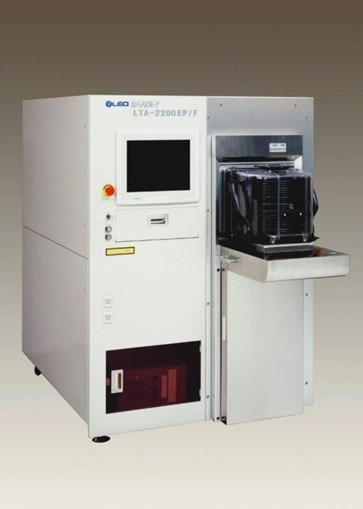
LTA series
- Features
-
- Temporal change of the carrier injected into the sample by laser beam is detected by microwave reflection power (μ-PCD method).
- By using the differential μ-PCD method, the life time of epi/diffusion wafers with low resistivity substrates can be measured.
- Usage
-
- Understanding contamination and defects during polishing, cleaning, oxidation, and diffusion processes for Si/SiC:bulk, epi, epi sub and SOI wafers, control of epi furnace, inspection when receiving/shipping, etc.
Magic mirror
Fine irregularities formed on mirror surfaces can be displayed with a clear image.
With the MIS series using the magic mirror principle, abnormalities in wafer surface shape can be easily detected.
Responsible Company: Kobelco Research Institute, Inc.
Measurement examples
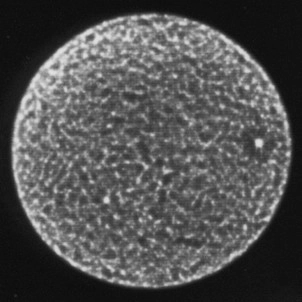
convex (black spots)
Product line-up
MIS series
- Features
-
- Slightly convex/concave surfaces, surface roughness, waviness, stepping, edge chipping, etc. can be observed on the monitor as a gray image.
- Automatic judgement is also possible by image processing.
- Usage
-
- Observation of surface roughness, convex/concave surfaces, polishing marks, edge chipping, etc. in the wafer production process
Example: post-grinding inspection (a defective wafer can be detected before polishing; fast measurement speed helps 100% inspection)
- Observation of surface roughness, convex/concave surfaces, polishing marks, edge chipping, etc. in the wafer production process
Contact Us
You can reach us by clicking the inquiry button.