Testing and analysis of semiconductor and manufacturing equipment
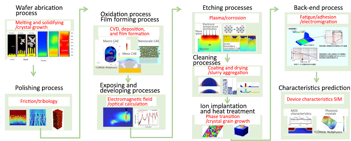
Wafer Production
Front-end Process
Back-end Process
“Analysis/evaluation technologies x material knowledge” supports semiconductor-related R&D!
Testing and analysis
Materials and components
- Physical properties evaluation of materials (from thin film to bulk material)
- Electric properties, thermal properties, magnetic properties, mechanical strength, etc.
- Analysis of deterioration under special environments
- Corrosive gas, chemicals, exposure to hydrogen, high to low temperature, etc.
- Trial production of materials and material reformation
- Special alloy materials, three dimensional modeling materials, etc.
- Process study of systemic control
- Trial production of products related to recycling
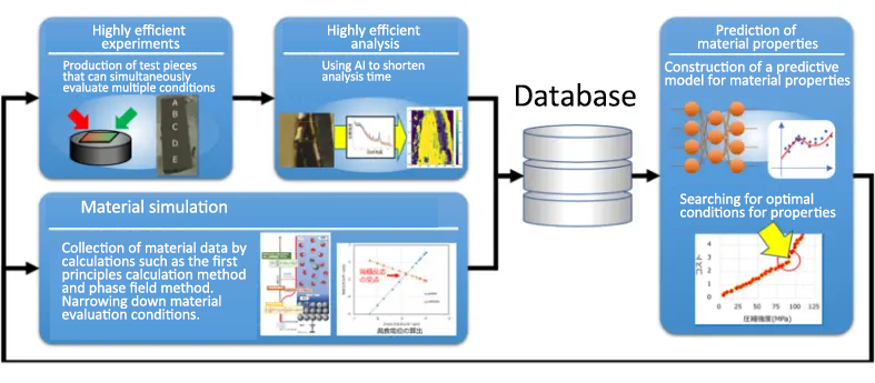
- Materials informatics
- Prediction of physical properties by machine learning
Semiconductor manufacturing equipment
- Corrosion and deterioration analysis of metals, ceramics, and resin parts
- Simulation and reproduction test of deterioration caused by various gases, plasma, chemicals, etc.
- Analysis of corrosion and deterioration mechanisms (physical analysis)
- Durability test of various parts, pipes, containers, etc.
- Strength and fracture tests under various high pressure gas environments
- Strength and fracture tests in high and low temperature environments
- Equipment-related evaluation
- Sliding test (friction and abrasion) under various conditions, vibration analysis
- Visualization test on flow of gases and liquids
Wafers, thin films, and devices
- Evaluation of various wafers
- Ultra-trace element analysis / Cleanliness Evaluation of Environmental Air in Clean Room
- Crystal defects on surface, structural defects
- Measurement of wafer flatness, edge shape, etc.
- Evaluation of thin film physical properties and structure
- Crystal structure analysis and surface analysis
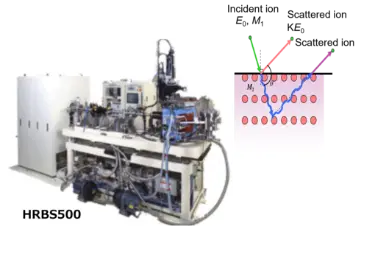
- High resolution analysis of thin films by HR-RBS
- Assessment of devices, implementing materials, etc.
- Assessment of bonding and strength
- *Fatigue strength of solder, bonding material, etc., and CAE collaboration
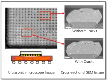
- Wide cross-section observation technique
- Failure analysis with OBIRCH, etc.
- Assessment of bonding and strength
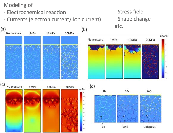
Simulation technologies that support semiconductor development
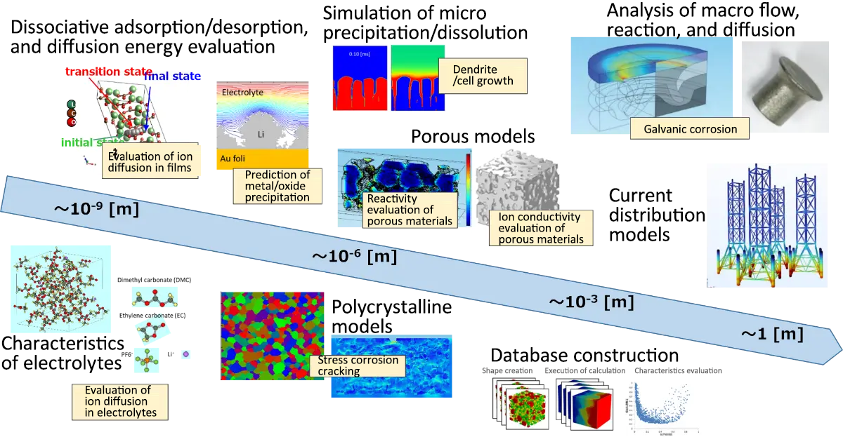
Multi-scale simulation
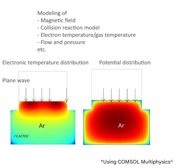
Plasma simulation
Corrosion simulation in gas phase and liquid phase
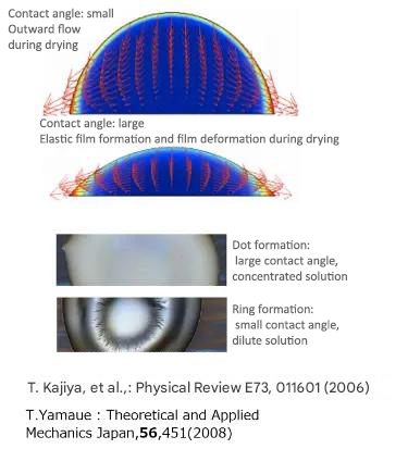
Solution drying and dot formation analysis
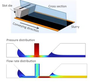
Die Coating Simulation
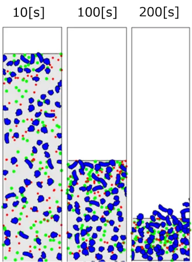
Simulation of slurry drying and particle aggregation
Contact Us
You can reach us by clicking the inquiry button.